Using electron microscopy and in-situ x-ray diffraction to understand solar cell manufacturing
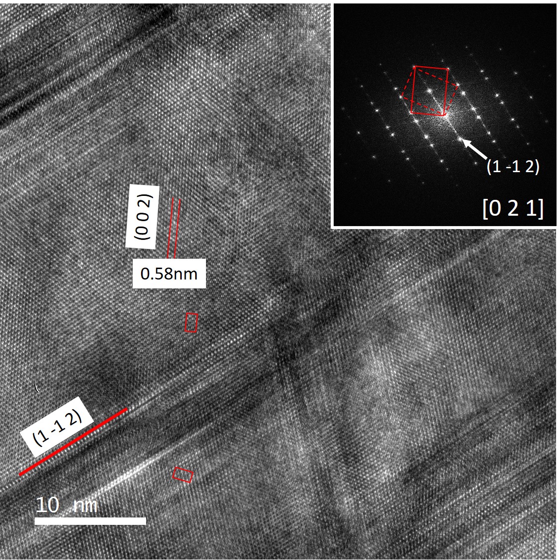
Lattice imaging and diffraction pattern (inset) for identification of specific grains in solar cells. This particular grains is Ag(Ga,In)Se2. 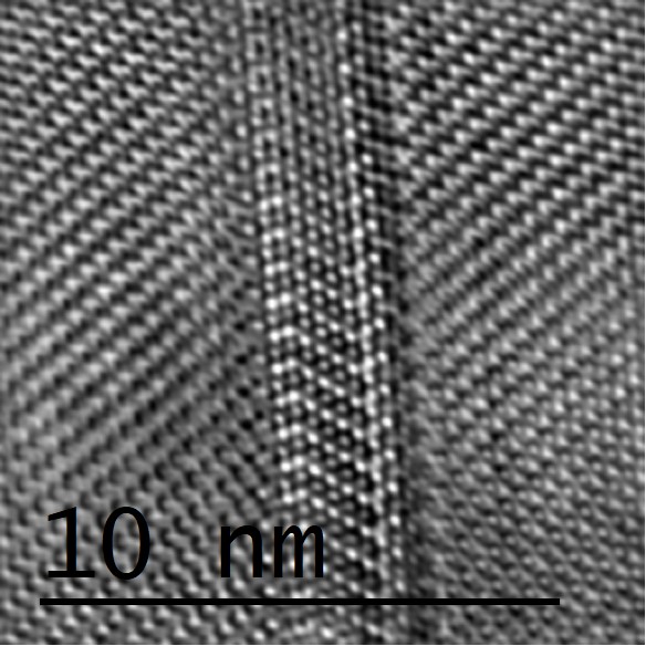
Rows of atoms observed using a high resolution transmission electron microscope. The breaks in crystalline pattern show here is typical of a twinning defect in a Cu2(Zn,Sn)S4 crystal which are detrimental to solar cell efficency. 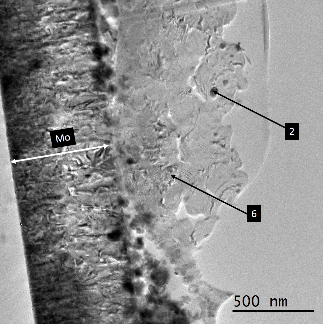
Overview of many crystals in the cross-section of a solar cell 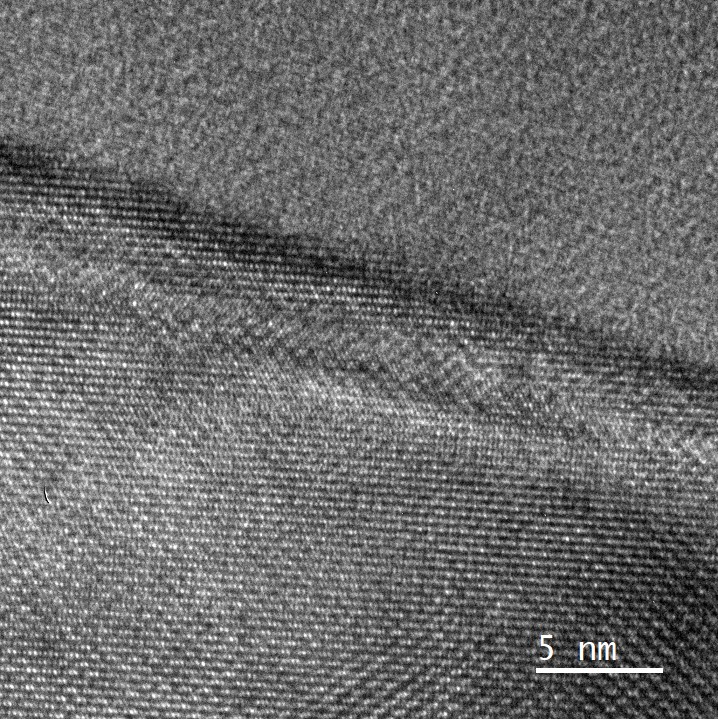
Lattice image of the interface between two crystals of Cu(Ga,In)Se2. 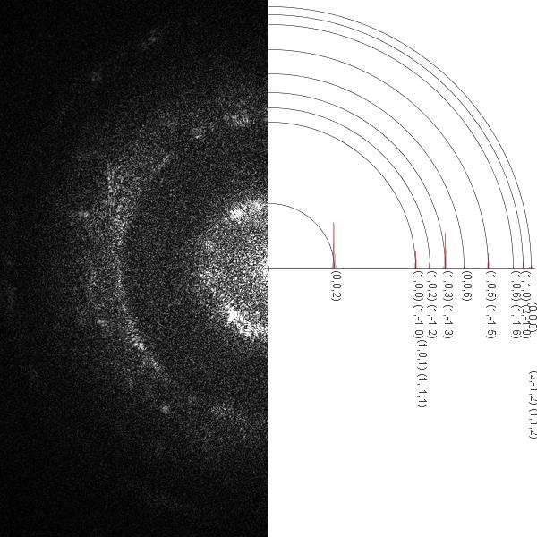
Phase identification using an electron diffraction pattern 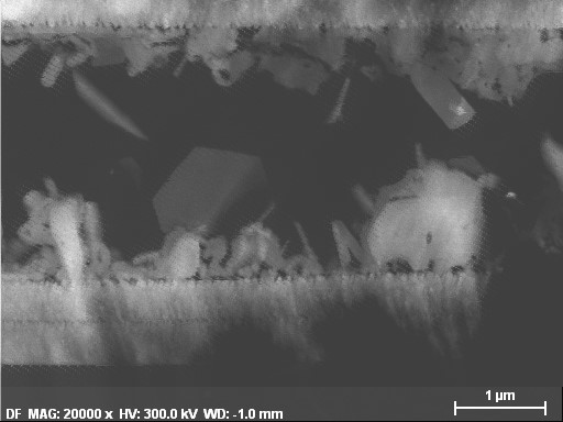
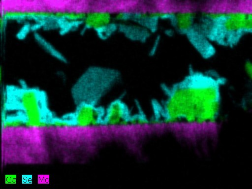
Elemental identification using energy dispersive x-rays 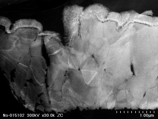
Scanning TEM image of a cross-section of a completed solar cell 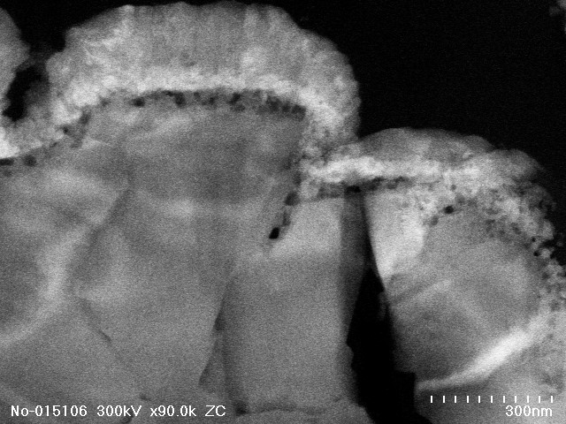
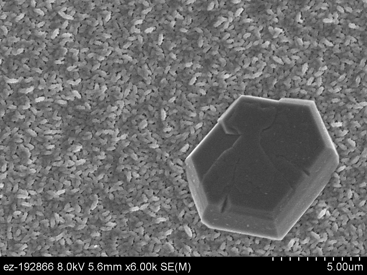
Cu2-xSe crystal grown on a bed of Cu(Ga,In)Se2. The hexagonal lattice structure of Cu2-xSe on the atomic level is reflected on the macro scale. 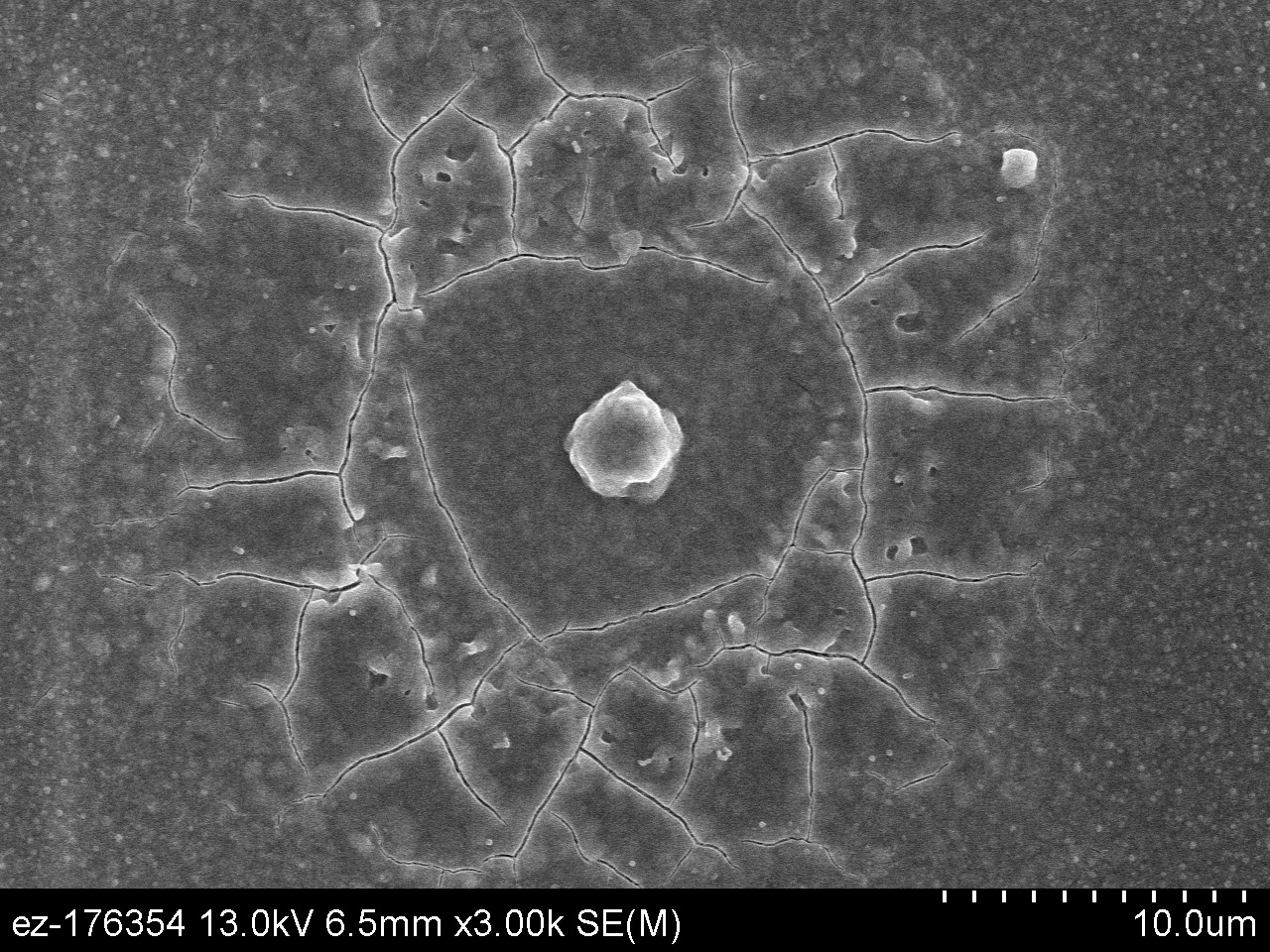
Cool looking contaminates 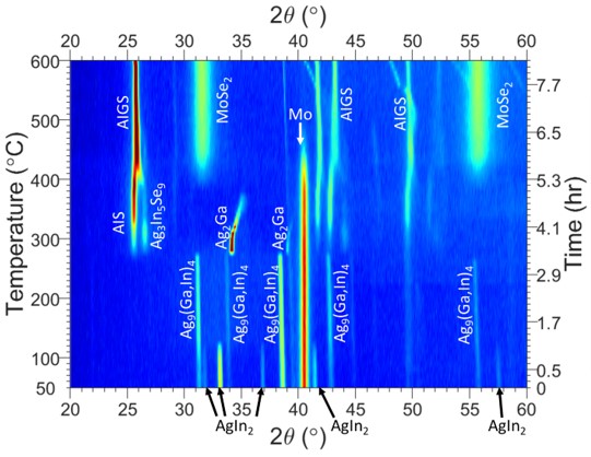
Derivation of reaction pathways during the fabrication of solar cells layers. Data visualization is semi automatically generated using custom Matlab scripts, allowing the scientist to focus on understanding results
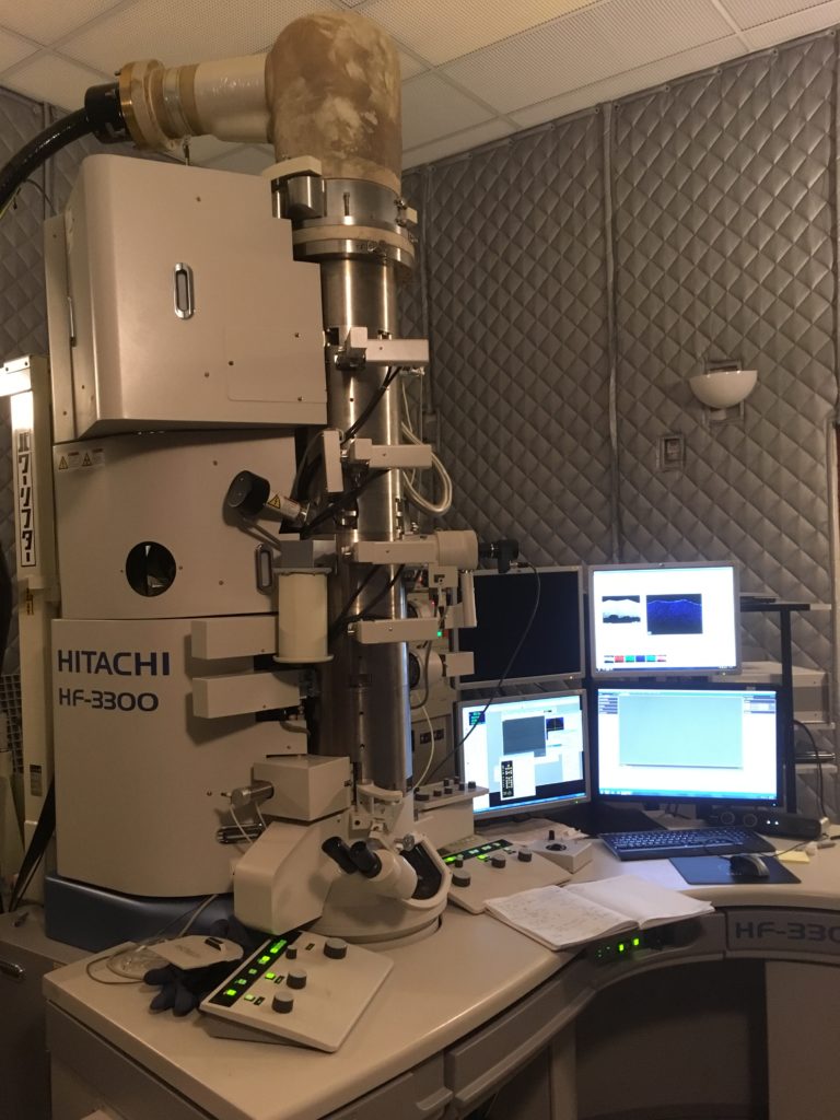
Hitachi HF-3300. A cold field emission high resolution and scanning transmission electron microscope with EDS, EELS, and many in-situ add-ons. 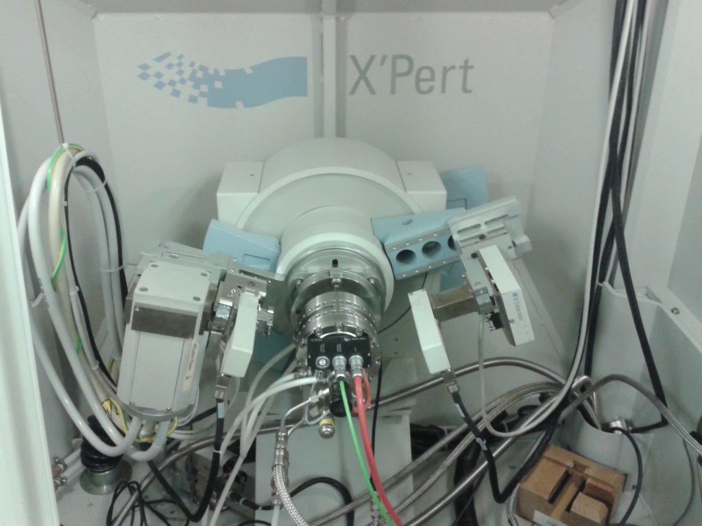
In-situ high temperature x-ray diffraction 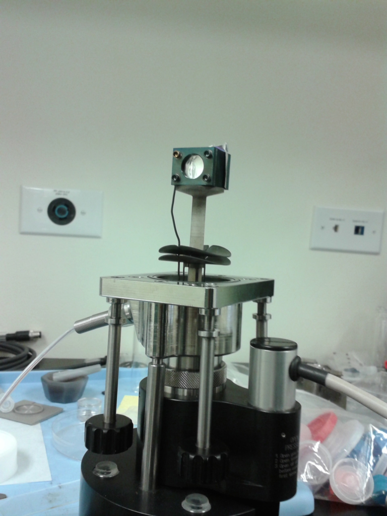
Custom reactor for observing solar cell formation 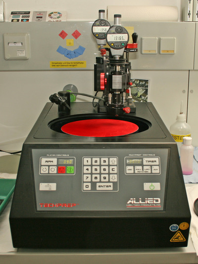

Mechanically polishing TEM samples down to 1 micron thickness before using Ar-ion milling to mill it down to 10-100nm